TXRF Spectrometer: ElvaX Thin Film Analysis
Understanding TXRF Technology
Total Reflection X-Ray Fluorescence differs fundamentally from conventional XRF through the geometry of X-ray incidence. While standard XRF directs X-rays at samples at typical angles (30-90 degrees), TXRF employs extremely shallow angles typically 0.05-0.5 degrees—below the critical angle for total external reflection on polished surfaces.
At these grazing angles, X-rays undergo total reflection at the sample surface, creating an X-ray standing wave in a thin surface layer only 5-10 nanometers deep. This phenomenon restricts excitation to the outermost surface atoms while virtually eliminating background signal from the substrate. The result is dramatically enhanced sensitivity specifically for surface elements and contaminants.
The shallow penetration depth makes TXRF ideal for analyzing surface contamination, thin film composition, and interfacial layers where conventional XRF's deeper penetration would overwhelm surface signals with substrate contribution. Applications requiring detection of trace metal contamination on wafer surfaces, thin coating characterization, or surface treatment verification benefit from TXRF's surface-specific sensitivity.
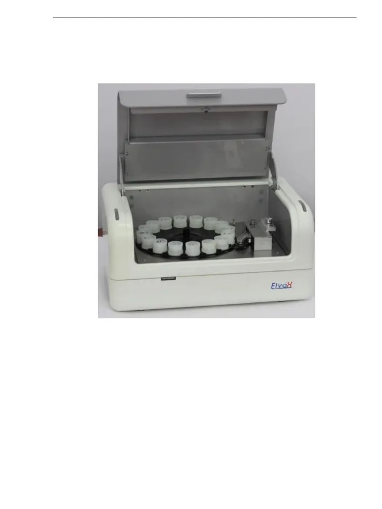
ElvaX TX 2000 Capabilities
The ElvaX TX 2000 spectrometer implements energy-dispersive X-ray fluorescence analysis in total reflection geometry, combining specialized hardware for grazing-incidence excitation with advanced detection systems optimized for ultra-low concentration measurements. The system enables quantitative analysis of surface contamination and thin film composition with exceptional sensitivity.
Elemental coverage spans sodium through uranium, detecting virtually all elements of interest for semiconductor manufacturing, materials science, and thin film applications. The wide elemental range enables comprehensive surface characterization identifying both expected constituents and unexpected contaminants in single measurements.
Detection limits reaching parts-per-billion or even parts-per-trillion levels for favorable element-matrix combinations provide sensitivity required for semiconductor wafer contamination control. This exceptional capability detects metal contamination at concentrations far below levels affecting device performance, enabling proactive quality control preventing defects before they impact production.
Semiconductor Wafer Analysis
Surface Contamination Detection
Semiconductor manufacturing demands extreme cleanliness—even trace metal contamination at parts-per-billion levels can cause device failures, reduced yields, or performance degradation. TXRF spectrometry provides the sensitivity required for detecting and quantifying these ultra-trace surface contaminants on silicon, silicon carbide, gallium arsenide, and sapphire wafers.
The technique monitors metal contamination including iron, copper, nickel, chromium, zinc, and other elements introduced during processing steps like wet chemical cleaning, deposition, etching, or handling. Regular TXRF analysis verifies process cleanliness, identifies contamination sources, and ensures wafer surfaces meet specifications before subsequent processing.
TXRF's non-destructive nature enables testing production wafers without compromising their use in device fabrication. This capability supports statistical process control monitoring contamination levels across production lots while preserving tested wafers for manufacturing, optimizing both quality assurance and material utilization.
Process Control and Troubleshooting
When semiconductor yields decline or device performance degrades, TXRF analysis helps identify root causes by detecting unexpected surface contamination. The comprehensive elemental coverage reveals contamination signatures pointing to specific process steps, equipment malfunctions, or material problems.
Routine TXRF monitoring establishes baseline contamination levels for healthy processes. Deviations from baselines trigger investigations before contamination reaches levels causing defects. This proactive approach prevents quality excursions and maintains stable, high-yield manufacturing.
Thin Film Composition Analysis
Coating Characterization
TXRF analyzes thin film composition and uniformity for coatings ranging from single nanometers to hundreds of nanometers thickness. Vapor-deposited metals, sputtered alloys, solution-applied coatings, and electroplated layers undergo compositional characterization revealing elemental ratios, detecting impurities, and verifying process control.
The surface-specific measurement distinguishes thin film composition from underlying substrates even when films are only nanometers thick—impossible with conventional XRF where substrate signals dominate. This capability enables quality control of ultra-thin functional coatings in electronics, optics, and advanced materials applications.
Multi-layer coating systems receive layer-by-layer analysis by combining TXRF with controlled etching or depth profiling techniques. Understanding compositional variations through coating thickness supports optimization of deposition processes and correlation of composition with functional properties.
Interface and Surface Treatment Verification
Surface treatments modifying chemical composition in near-surface regions undergo verification through TXRF analysis. Cleaning processes, plasma treatments, chemical conversions, and surface modification procedures change surface elemental composition in ways TXRF detects and quantifies.
The technique verifies that surface treatments achieved intended effects—contaminant removal after cleaning, oxide thickness after oxidation, incorporation of dopants during surface modification. Process validation through TXRF measurement ensures treatments meet specifications supporting subsequent processing or final product requirements.
Advanced Materials Research
Nanomaterial Characterization
Nanotechnology research employs TXRF for analyzing nanoparticle composition, surface functionalization, and contamination. Nanoparticle suspensions deposited on reflective substrates undergo TXRF analysis revealing elemental composition with minimal sample preparation. The technique supports quality control of synthesized nanomaterials and characterization of surface coatings on nanoparticles.
Two-dimensional materials like graphene, transition metal dichalcogenides, and other atomic-scale films receive compositional analysis through TXRF. The extreme surface sensitivity matches perfectly with these materials where the entire sample consists of surface atoms. Dopant incorporation, contamination detection, and intercalation verification benefit from TXRF's surface-specific capability.
Catalyst and Functional Surface Analysis
Catalysis research uses TXRF to characterize catalyst surface composition and metal loading. Supported metal catalysts, nanoparticle catalysts, and surface-modified catalytic materials undergo analysis revealing active metal content, detecting contaminants, and monitoring catalyst degradation during use.
Functional coatings for optical, electronic, or catalytic applications receive compositional verification through TXRF. The technique ensures that intended elemental compositions were achieved during deposition, identifies process variations affecting performance, and troubleshoots coating failures through contamination detection.
Sample Preparation and Measurement
Substrate Requirements
TXRF requires flat, polished substrates enabling total X-ray reflection. Silicon wafers naturally meet requirements. Other samples may require deposition onto suitable reflective substrates—typically high-purity silicon, quartz, or polished glass. Liquid samples evaporate onto reflectors, powders suspend and deposit, and irregular solids may require digestion and deposition.
This sample preparation, while adding steps compared to conventional XRF, enables TXRF's exceptional sensitivity by creating ideal measurement geometry. For applications requiring ultra-trace detection, the preparation investment delivers unmatched analytical capability.
Quantification Methods
TXRF quantification typically employs internal standards added to samples before deposition. The standard element's known concentration enables accurate quantification of detected elements regardless of exact sample amount deposited. This approach eliminates matrix effects and geometric uncertainties affecting other techniques.
For wafer contamination analysis, comparison to calibrated reference wafers or vapor-deposited standards provides quantitative results. The quantification achieves accuracy sufficient for semiconductor process control and materials specification verification.
Advantages and Limitations
TXRF Strengths
Exceptional surface sensitivity provides orders-of-magnitude better detection limits than conventional XRF for surface analysis. Parts-per-billion and parts-per-trillion detection enables applications impossible with other techniques. The minimal sample requirements—nanogram quantities—preserve valuable materials while providing comprehensive elemental data.
Non-destructive analysis preserves samples for additional testing or use. Multi-element capability delivers complete elemental profiles from single measurements. The small excitation area enables local analysis and contamination mapping across sample surfaces.
Practical Considerations
TXRF requires flat, polished substrates limiting direct analysis of rough or irregular samples. Sample preparation through deposition adds workflow steps compared to conventional XRF. The surface-specific measurement analyzes only outermost nanometers—beneficial for surface analysis but unsuitable for bulk composition determination.
The technique works best with solid substrates at room temperature. Liquid analysis requires evaporative deposition. Light element detection, while possible, faces challenges similar to conventional XRF requiring specialized conditions like vacuum or helium atmosphere.
Conclusion
TXRF spectrometry through the ElvaX TX 2000 platform delivers specialized analytical capability for thin film and surface contamination analysis at sensitivity levels impossible with conventional techniques. The grazing-incidence total reflection geometry restricts excitation to outermost nanometers while eliminating substrate background, achieving parts-per-billion detection essential for semiconductor manufacturing, advanced materials research, and demanding thin film applications.
For laboratories requiring ultra-trace surface contamination detection, comprehensive thin film characterization, or surface treatment verification at ultimate sensitivity, TXRF represents the optimal analytical approach. The ElvaX implementation provides accessible total reflection XRF capability supporting quality control, research, and development across semiconductor, nanotechnology, and advanced materials industries.
Understanding TXRF's unique strengths—exceptional surface sensitivity, minimal sample requirements, non-destructive analysis—along with practical requirements for flat substrates and sample preparation enables informed decisions about when this specialized technique delivers optimal value. For applications where surface composition at ultra-trace levels determines success, TXRF spectrometry provides unmatched analytical power.
Related posts
-
 XRF Spectrometer: ElvaX Metal Analysis Solutions
Metal analysis drives quality control, material verification, and production excellence across manufacturing...Einzelheiten
XRF Spectrometer: ElvaX Metal Analysis Solutions
Metal analysis drives quality control, material verification, and production excellence across manufacturing...Einzelheiten -
 Portable XRF Spectrometer: ProSpector 3 High Speed
Speed defines competitive advantage in modern materials testing. The ProSpector 3 portable XRF spectrometer...Einzelheiten
Portable XRF Spectrometer: ProSpector 3 High Speed
Speed defines competitive advantage in modern materials testing. The ProSpector 3 portable XRF spectrometer...Einzelheiten -
 XRF Spectrometers: 2026 Model Selection Guide
Selecting the right XRF spectrometer requires matching instrument capabilities to your specific analytical...Einzelheiten
XRF Spectrometers: 2026 Model Selection Guide
Selecting the right XRF spectrometer requires matching instrument capabilities to your specific analytical...Einzelheiten -
 Portable XRF Spectrometer: Field Applications
Portable XRF spectrometers have transformed materials testing by bringing laboratory-quality elemental analysis...Einzelheiten
Portable XRF Spectrometer: Field Applications
Portable XRF spectrometers have transformed materials testing by bringing laboratory-quality elemental analysis...Einzelheiten -
 Handheld XRF Spectrometer: ProSpector 2
The ProSpector 2 handheld XRF spectrometer represents proven technology trusted by thousands of users worldwide for...Einzelheiten
Handheld XRF Spectrometer: ProSpector 2
The ProSpector 2 handheld XRF spectrometer represents proven technology trusted by thousands of users worldwide for...Einzelheiten